TPS54202DDCR is a high-performance DC-DC switching regulator from Texas Instruments (TI), belonging to the PMIC (Power Management Integrated Circuit) series. This device, with its extensive functional characteristics and excellent performance, is highly favored in power management applications. This article will delve into the technical features of TPS54202DDCR to provide readers with a better understanding and application of this product.
TPS54202DDCR is a 2A synchronous buck converter with an input voltage range of 4.5V to 28V. This means it can handle input voltages from 4.5V to 28V and deliver a maximum current of 2A. This wide input voltage range makes it suitable for various applications, such as 2V and 24V distributed power bus supplies, audio equipment, STBs (Set-Top Boxes), DTVs (Digital Televisions), and other consumer appliances.
TPS54202DDCR integrates two switching FETs (Field-Effect Transistors) and features internal loop compensation and a 5ms internal soft-start function. These features significantly reduce the number of external components, simplify circuit design, and enhance system reliability and stability. With a SOT-23 package, TPS54202DDCR achieves high power density while occupying minimal space on the printed circuit board (PCB), making it ideal for applications with stringent space requirements.
Another notable feature of TPS54202DDCR is its advanced Eco-mode. This mode maximizes light-load efficiency and reduces power loss through pulse-skipping technology. This characteristic makes TPS54202DDCR particularly outstanding in applications with high energy efficiency requirements, such as battery-powered devices.
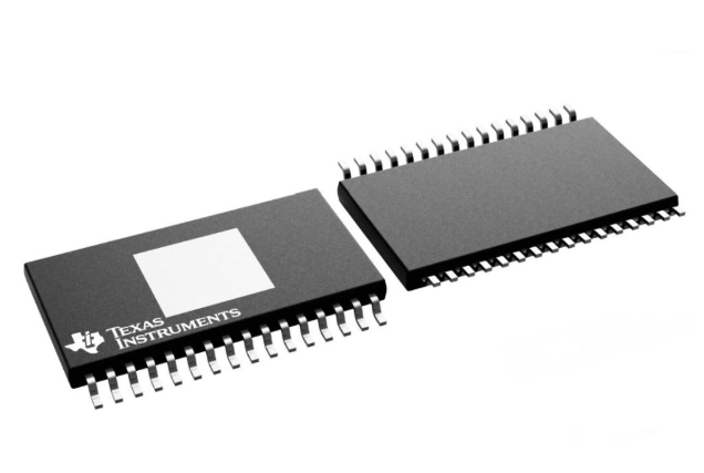
To reduce electromagnetic interference (EMI), TPS54202DDCR incorporates spread-spectrum operation. By adjusting the switching frequency, spread-spectrum operation effectively lowers EMI and improves the system's electromagnetic compatibility. This is crucial for applications that need to meet strict electromagnetic compatibility standards.
TPS54202DDCR also boasts multiple protection features to ensure stable system operation. Cycle-by-cycle current limiting on the high-side MOSFET protects the converter from overload conditions and prevents current runaway. Additionally, freewheeling current limiting on the low-side MOSFET further enhances protection capabilities. If the overcurrent condition persists beyond a preset time, TPS54202DDCR triggers hiccup mode protection to further safeguard the circuit.
TPS54202DDCR also features overvoltage protection and thermal shutdown functions. These functions automatically shut down the converter when the voltage is too high or the temperature is too high, thereby protecting the system from damage.
TPS54202DDCR operates at a switching frequency of 500kHz, which is relatively high and helps reduce the size of the output capacitor and improve the system's dynamic response performance. The optimized internal compensation network further simplifies the design of the control loop and reduces the number of external components.
In conclusion, TPS54202DDCR showcases exceptional performance in power management applications due to its wide input voltage range, high power density, advanced Eco-mode, spread-spectrum operation, multiple protection features, and optimized internal compensation network. These features make TPS54202DDCR an ideal choice for designing efficient and reliable power management systems.


