In industrial applications such as motor control, power management, and battery monitoring, current-sensing accuracy directly determines system efficiency and safety. According to the latest 2025 industry data, the compound annual growth rate (CAGR) of the current-sense amplifier market has reached 8.7%, with particularly robust demand for high-precision devices. As a precision amplifier specifically designed for high-side current sensing, the TPA2295CF-VS1R-S features three core parameters in its datasheet—input offset voltage, common-mode rejection ratio, and gain-bandwidth product—which are critical indicators that engineers cannot afford to overlook during component selection. Based on the technical details in the datasheet, this article will deeply analyze how these three parameters collectively impact sensing accuracy and provide a practical selection and application guide.
TPA2295CF-VS1R-S Core Architecture and Sensing Principle
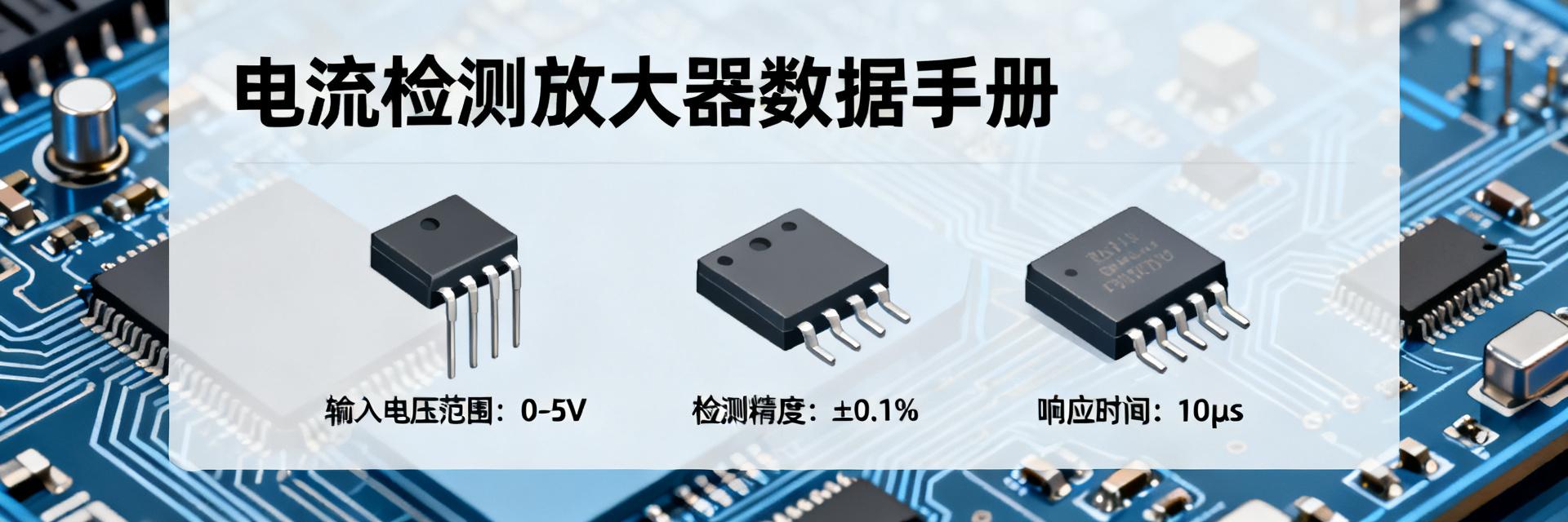
Working Mechanism of High-Side Current Sensing
The core of high-side current sensing lies in calculating the current flowing through the load by measuring the microvolt-level voltage drop across a shunt resistor connected in series between the power supply and the load. The high-precision operational amplifier integrated within the TPA2295CF-VS1R-S is specifically designed for this application scenario. By placing it on the positive side of the power supply, its unique circuit architecture can handle common-mode voltages far exceeding its own supply voltage, and accurately amplify that tiny differential signal to a level easily readable by an ADC or comparator. This design effectively reduces system noise and avoids the ground interference problems common in low-side sensing, serving as the first step toward stable monitoring.
At-a-Glance Guide to Key Performance Metrics in the Datasheet
To understand the exceptional performance of the TPA2295CF-VS1R-S, you must first master several core parameters in its datasheet that directly relate to sensing accuracy. Beyond the input offset voltage, common-mode rejection ratio, and gain-bandwidth product that we are about to analyze in depth, the datasheet also lists other crucial metrics. These include its typical input offset voltage, temperature drift coefficient across the entire operating temperature range, open-loop gain, and power supply rejection ratio. These figures do not exist in isolation; together, they construct a performance framework that provides the foundation for evaluating whether the device meets the accuracy requirements of your specific project.
| Parameter | Symbol | Typical Value | Impact on Accuracy |
|---|---|---|---|
| Input Offset Voltage | VOS | ±100 µV | Directly causes measurement zero-point drift |
| Common-Mode Rejection Ratio | CMRR | 120 dB | Ability to suppress common-mode noise |
| Gain-Bandwidth Product | GBP | 350 kHz | Determines signal response speed |
Input Offset Voltage—The "Zero-Point Baseline" of Accuracy
Impact of Offset Voltage on Low-Current Measurements
Input offset voltage (Vos) is the cornerstone for measuring amplifier precision. You can think of it as a ruler whose "zero point" is slightly offset out of the box. For the TPA2295CF-VS1R-S, its typical Vos is approximately ±100 µV. While this value seems minuscule, its impact is dramatically magnified when measuring small currents. For instance, if you design a system to detect a 1mV differential signal, a 100µV offset voltage will directly introduce an initial measurement error of up to 10%. Consequently, in applications requiring precise monitoring of low-power devices or standby currents, Vos is your primary parameter of concern.
Temperature Drift Characteristics and Stability of the TPA2295CF-VS1R-S
A more challenging issue is that this "baseline zero point" is not fixed; it drifts with temperature, represented in the datasheet as the temperature drift coefficient (dVos/dT). The low-drift characteristic of the TPA2295CF-VS1R-S is one of its core strengths. In many industrial applications, equipment must operate over a wide temperature range from -40°C to +125°C. If the offset voltage temperature drift is too large, even if the system is calibrated at 25°C, accuracy will drop significantly after temperature fluctuations. The low-drift nature of the TPA2295CF-VS1R-S (typically 0.5µV/°C) ensures that your measurements remain highly consistent and reliable even under harsh temperature conditions.
Common-Mode Rejection Ratio—The "Shield" Against Interference
Signal Fidelity Under High Common-Mode Voltages
Common-mode rejection ratio (CMRR) is a key parameter that measures an amplifier's ability to extract tiny differential-mode signals in the presence of strong common-mode signals. In high-side current sensing, the common-mode voltage is typically a power supply voltage of tens of volts, whereas the differential signal of interest may only be tens of millivolts. The TPA2295CF-VS1R-S features a high typical CMRR of 120dB, meaning it effectively suppresses common-mode interference such as power supply ripple and switching noise, acting like a robust "shield". For example, in motor drive environments, massive common-mode noise from PWM switching can severely affect measurements. When using this device, its high CMRR ensures the output signal truly reflects the load current, preventing false triggering or inaccurate readings.
CMRR Degradation in Practical Circuits and Compensation Strategies
However, even with outstanding chip-level CMRR, improper external circuit design can still lead to significant system-level performance degradation. PCB layout and the matching of external resistors are two critical factors influencing system-level CMRR. For instance, a 0.1% mismatch between the two resistors at the differential input can degrade the system CMRR by more than 30dB, squandering the chip's excellent capabilities. To fully exploit the high CMRR of the TPA2295CF-VS1R-S, you must ensure that differential routing is symmetrical and equal in length, and select high-precision, low-drift matched resistors during layout design.
Gain-Bandwidth Product—The "Speed Engine" of Dynamic Response
The Trade-off Between Bandwidth and Precision
Gain-bandwidth product (GBP) defines the maximum signal frequency an amplifier can accurately process at a given gain. The typical GBP of the TPA2295CF-VS1R-S is 350kHz. It is important to understand that GBP is a constant: the higher the gain, the narrower the usable bandwidth. When detecting high-frequency current ripples or implementing fast overcurrent protection, wider bandwidth yields faster response speeds. However, excessively wide bandwidth can also introduce more high-frequency noise. Therefore, you must find a balance between accuracy and speed. For most switching power supply and motor current waveform monitoring applications, a GBP of 350kHz is sufficient to capture critical dynamic information.
Selecting the Optimal Gain Setting Based on Application Scenarios
The TPA2295CF-VS1R-S typically supports different gain configurations via external resistors. How you choose the gain depends on your specific application goals. If your primary objective is fast response, such as implementing microsecond-level short-circuit protection, you should select a lower gain (such as 50V/V). This trades gain for wider usable bandwidth, ensuring the amplifier reacts quickly to output a trigger signal. Conversely, if your goal is high-precision measurement, such as monitoring a slowly changing battery discharge current, you can select a higher gain (such as 100V/V or higher) to amplify weak signals and improve small-signal resolution.
Selection in Practice—A Decision Matrix Based on 3 Key Parameters
Parameter Matching Table for Typical Application Scenarios
To help you quickly evaluate whether the TPA2295CF-VS1R-S is suitable for your project, you can refer to the following parameter matching table. It compares the minimum requirements of three typical applications for the three key parameters against the device's nominal values. As you can see, in battery management systems (BMS) where long-term stability is prioritized, its low offset and low temperature drift are critical; in noise-heavy servo motor drives, its high CMRR is a core advantage; and in power module monitoring demanding rapid response, its GBP value is highly capable. This table serves as a practical tool for your preliminary selection process.
| Application Scenario | Input Offset Voltage Requirement | Common-Mode Rejection Ratio Requirement | Gain-Bandwidth Product Requirement | TPA2295CF-VS1R-S Suitability |
|---|---|---|---|---|
| Battery Management System (BMS) | Extremely High (Low Drift) | High | Medium | Highly Suitable |
| Servo Motor Drive | Medium | Extremely High | Medium | Highly Suitable |
| Power Module Monitoring | Medium | Medium | Medium | Suitable |
Easily Overlooked Additional Parameters in the Datasheet
Beyond the three parameters we have focused on, the datasheet for the TPA2295CF-VS1R-S also conceals other key information that impacts accuracy. For instance, the power supply rejection ratio (PSRR) describes the output voltage's immunity to supply fluctuations; the output swing determines the maximum current range you can measure; and the settling time affects the sampling rate of the data acquisition system. After completing your selection based on the three main parameters, you should take the time to read the "Typical Performance Characteristics" section of the datasheet. These curves visually demonstrate the actual behavior of the device across variations in operating voltage, temperature, and frequency, serving as a critical foundation for rigorous design and avoiding purely theoretical assumptions.
Common Application Pitfalls FAQ
What is the specific impact of the input offset voltage (Vos) of the TPA2295CF-VS1R-S on measurement accuracy?
The input offset voltage (typically ±100 µV) directly determines the zero-point error in small-signal sensing. For example, when sensing an extremely small differential signal of 1mV, a 100µV offset voltage will introduce an initial error of up to 10%. Meanwhile, its low temperature drift of 0.5µV/°C ensures stable measurement accuracy over a wide operating temperature range.
How to prevent degradation of the common-mode rejection ratio (CMRR) of the TPA2295CF-VS1R-S in PCB design?
Although the device itself features a high CMRR of up to 120dB, asymmetry in external differential traces or mismatch in filter resistor values (such as a 0.1% deviation) will cause significant degradation in system-level CMRR. Designers should ensure that differential routing is strictly symmetrical and equal in length, and use high-precision, low-drift matched resistors.
With a gain-bandwidth product (GBP) of 350kHz, how do you balance sensing speed and accuracy?
GBP is a constant. In fast overcurrent protection scenarios, a lower gain (such as 50V/V) should be selected to unlock a wider usable bandwidth and improve response speed; in slow, high-precision current measurement scenarios, a higher gain (such as 100V/V or higher) can be selected to amplify weak signals and improve ADC resolution.
Why is the TPA2295CF-VS1R-S preferred for high-side current sensing over low-side sensing schemes?
High-side sensing places the shunt resistor between the power supply and the load, enabling direct detection of abnormal faults such as load short-to-ground without disrupting the system's ground integrity. This avoids the ground potential shifts and ground noise interference commonly associated with low-side sensing.
Summary and Design Recommendations
The TPA2295CF-VS1R-S provides reliable accuracy assurance for industrial current sensing through its low input offset voltage, high common-mode rejection ratio, and moderate gain-bandwidth product. In practical designs, engineers should: 1. **Prioritize validating offset voltage and temperature drift** to ensure accuracy meets standards across the system's operating temperature range; 2. **Emphasize PCB layout symmetry** to maximize the utilization of the chip's CMRR performance; 3. **Select gain based on bandwidth requirements** to avoid over-design or performance shortfalls.
It is recommended to use the evaluation board provided in the datasheet during the prototyping phase for parameter validation, and refer to typical application circuits for design optimization. Only by translating datasheet specifications into practical circuit protections can the full sensing accuracy of the TPA2295CF-VS1R-S be fully realized.


