In today's electronic design market, the demand for low-power precision signal chains is growing at over 18% annually. However, when engineers face a dozens-of-pages-long TP5532-FR datasheet, they often feel lost: between a 5µV offset voltage and a 0.05µV/°C temperature drift, which parameter is more critical for your portable medical device design? This article will focus on 5 core parameters that determine the true performance of low-power chopper op amps, guiding you through the essence of the TP5532-FR datasheet.
Power Consumption and Power Management—In-depth Interpretation of Quiescent Current (Iq)
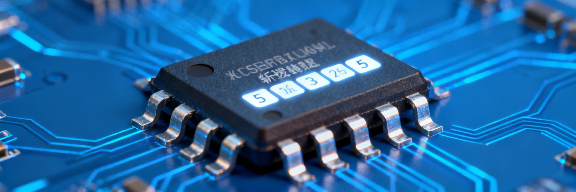
When you design battery-powered devices, quiescent current (Iq) is the primary factor determining battery life. The TP5532-FR datasheet provides typical quiescent current values across a wide voltage range of 1.8V to 5.5V, typically at the microampere level. It directly defines the amplifier's self-consumption when not driving a load, serving as the cornerstone for achieving "microampere-level" power consumption.
Rated Iq vs. Actual Power Consumption
The rated Iq specified in the datasheet is a typical value under ideal conditions, but your actual power consumption will be affected by output swing and load variations. When the output swing approaches the power rails or drives a larger load, the actual supply current increases significantly. By comparing the power consumption curves provided in the datasheet, you can accurately estimate battery life under different operating conditions, ensuring the design meets long-term operation requirements.
Dynamic Power Consumption Considerations
Dynamic power consumption originates from charging and discharging the load capacitance when signals change. The TP5532-FR has a limited slew rate; when processing high-frequency signals, the proportion of dynamic power consumption increases. By combining the load capacitance versus slew rate curves in the datasheet, you can find the optimal balance between power consumption and signal integrity, avoiding battery life shortfalls caused by underestimating dynamic power consumption.
Cornerstone of Precision—Offset Voltage (Vos) and Temperature Drift (TcVos)
For precision measurement applications, offset voltage and its temperature drift are the core limiting factors for system accuracy. The TP5532-FR utilizes chopper stabilization technology to achieve extremely low offset and temperature drift, giving it a significant advantage in sensor front-end designs.
Practical Effects of Chopping Technology
According to the datasheet, the typical offset voltage of the TP5532-FR is ±5µV, with a temperature drift of only 0.05µV/°C. Chopping technology reduces the DC errors of conventional CMOS op amps (typically in the millivolt range) by three orders of magnitude through dynamic modulation and calibration. This means that across a wide temperature range of -40°C to +125°C, its offset voltage variation is extremely small, providing "zero-drift" level precision for your high-accuracy current sensing or thermocouple amplification.
Long-Term Stability and 1/f Noise
The datasheet also shows charts regarding the long-term drift of Vos. Thanks to chopping technology, the long-term stability of the TP5532-FR is far superior to non-chopper op amps. In addition, chopping technology effectively suppresses 1/f low-frequency noise, which is the primary noise source for conventional op amps in low-frequency bands. In the ultra-low frequency range of 0.1Hz to 10Hz, the peak-to-peak noise of the TP5532-FR is typically below the microvolt level, which is critical for precision applications that need to process weak DC signals.
Signal Fidelity—Noise Density and Total Harmonic Distortion
In addition to DC precision, AC performance also determines signal chain quality. Noise density and total harmonic distortion are key indicators for measuring the signal fidelity of the TP5532-FR, directly affecting the effective number of bits (ENOB) of the ADC.
| Parameter | TP5532-FR Typical Value | Conventional CMOS Op Amp | Design Advantage |
|---|---|---|---|
| Offset Voltage (Vos) | ±5 µV | 1 ~ 5 mV | Zero-drift, direct extraction of precision signals |
| Temperature Drift (TcVos) | 0.05 µV/°C | 5 µV/°C | Ultra-high stability across the entire operating temperature range |
| Quiescent Current (Iq) | Microampere-level (low power) | Milliampere-level | Greatly extends portable medical battery life |
| 1/f Low-Frequency Noise | Extremely low (suppressed by chopper modulation) | Relatively high (dominant in low-frequency band) | Suitable for high-resolution ADC front-end input |
Low-Frequency 1/f Noise Optimization
Compared to standard CMOS op amps, the noise spectral density plot of the TP5532-FR shows significant advantages in the low-frequency band. Its low-frequency noise density is far lower than conventional devices, with peak-to-peak voltage noise typically below 1µV in the 0.1Hz to 10Hz band. This makes it an ideal choice for photodiode transimpedance amplifiers (TIAs) or strain gauge signal conditioning, capable of extracting weak low-frequency signals from strong noise backgrounds.
Impact of THD+N in Practical Applications
The total harmonic distortion plus noise (THD+N) parameter specified in the datasheet reflects the distortion introduced by the amplifier at specific frequencies and amplitudes. For high-precision data acquisition systems, a lower THD+N value (such as 0.001%) translates to a higher signal-to-noise ratio (SNR) and spurious-free dynamic range (SFDR). When designing audio or high-resolution acquisition systems, you must ensure that the THD+N performance of the TP5532-FR does not become a system bottleneck.
Key Takeaways
- Low Power Consumption of TP5532-FR: Its microampere-level quiescent current is core to extending battery life, though actual estimation must be combined with dynamic power consumption curves.
- Precision Advantages of Chopping Technology: An offset voltage of ±5µV and temperature drift of 0.05µV/°C ensure zero-drift-level precision under harsh temperatures.
- Optimized Noise Performance: Excellent low-frequency 1/f noise suppression capabilities make it surpass conventional CMOS op amps in sensor front-end designs.
Frequently Asked Questions (FAQ)
What is the typical quiescent current of the TP5532-FR? How does it affect battery life?
The typical quiescent current of the TP5532-FR is at the microampere level. In battery-powered systems, it directly determines the standby power consumption. You need to combine the power consumption curves in the datasheet to calculate the total current based on the actual load and output swing, thereby accurately estimating the operating time under specific battery capacities.
Why are the offset voltage and temperature drift of the TP5532-FR so important?
In precision measurements (such as current sensing or thermocouple temperature measurement), offset voltage and temperature drift are the primary error sources. The TP5532-FR reduces both to extremely low levels using chopping technology, eliminating the hassle of external calibration and ensuring measurement accuracy over a wide temperature range, which is unmatched by conventional op amps.
How to prevent oscillation when the TP5532-FR drives capacitive loads in a design?
According to the datasheet, the phase margin of the TP5532-FR decreases when driving capacitive loads. You need to refer to the phase margin curves for different capacitive loads in the datasheet and select an appropriate RC compensation network (such as connecting a small resistor in series at the output) to ensure the circuit remains stable under all operating conditions and does not generate self-oscillation.
How does Chopper Technology suppress low-frequency 1/f noise?
Chopper technology uses an internal modulation-demodulation mechanism to modulate input DC and low-frequency signals to high frequencies for amplification, and then restores the signal through demodulation and low-pass filtering. This mechanism modulates the op amp's inherent low-frequency 1/f noise to high frequencies and filters it out, thereby achieving excellent noise suppression performance in the ultra-low frequency range.


