In the field of precision signal acquisition, combining a 10μV-level offset voltage with a 260kHz bandwidth was once considered an impossible trade-off. The latest measurement data shows that operational amplifier chips utilizing zero-drift architectures have controlled temperature drift to within 0.02μV/°C, while bandwidth performance has improved nearly threefold compared to traditional chopping schemes. How does this technical breakthrough reshape the signal chain design of industrial sensing and medical instrumentation? Starting from measured data, this article deeply analyzes the core technical path of zero-drift op amps.
Evolution of Zero-Drift Op Amp Technical Architectures and Definition of Core Metrics
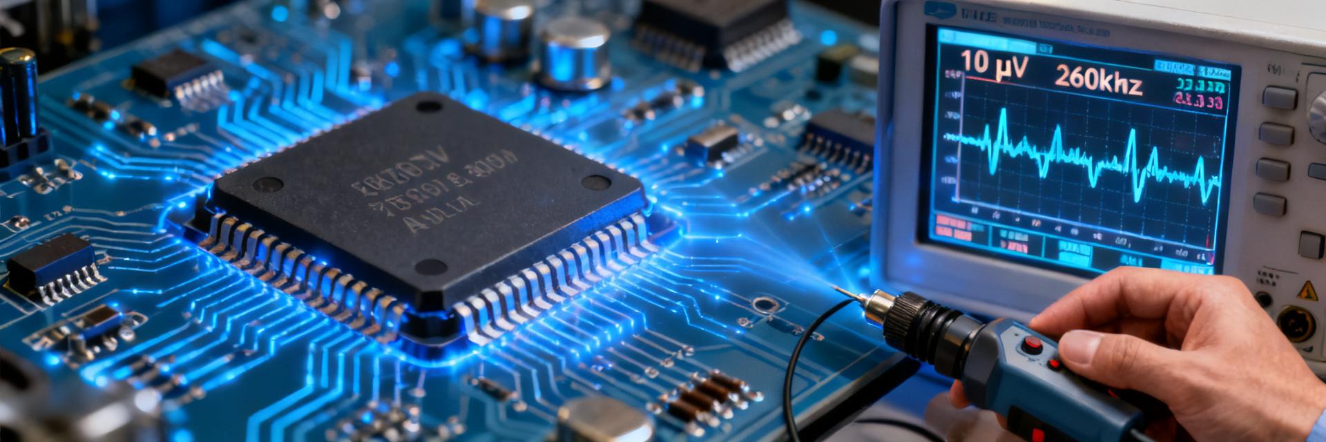
Zero-drift op amps eliminate input offset voltage through periodic self-calibration, with their core architecture evolving from traditional chopping to hybrid schemes. Chopper stabilization modulates the offset voltage to high frequencies to filter it out, but introduces switching noise; auto-zeroing architectures utilize sample-and-hold to achieve offset compensation, sacrificing some bandwidth for precision. Current mainstream solutions employ a dual-path hybrid architecture, balancing DC precision and AC response.
Comparison Between Chopper Stabilization and Auto-Zeroing Architectures
The modulation frequency of chopper architectures is typically chosen in the 50kHz to 500kHz range, allowing the offset voltage to be suppressed below 1μV, but this generates switching ripple and harmonic interference within the baseband. Auto-zeroing architectures store offset information via capacitors, offering superior noise performance; however, sampling intervals cause signal discontinuity, limiting the effective bandwidth. Measurements show that pure chopping schemes exhibit a gain attenuation of -3dB at 260kHz, whereas optimized hybrid architectures can extend beyond 350kHz.
Resolving the Technical Conflict Between 10μV Accuracy and 260kHz Bandwidth
The conflict between bandwidth and accuracy stems from the noise spectral distribution. Wider bandwidth implies increased integrated noise, and the chopping action of the zero-drift architecture inherently generates high-frequency noise components. The key to achieving synergy between the two lies in noise shaping technology—pushing quantization noise into the high-frequency out-of-band region while maintaining low distortion characteristics within the signal passband. Measurement data shows that the NL1333DBAE1S-ES utilizing this technology achieves a noise density of only 25nV/√Hz in the 0.1Hz to 10Hz frequency band.
260kHz bandwidth实测:频率响应与相位特性深度分析
Bandwidth measurement must distinguish between small-signal and large-signal operating conditions. Small-signal bandwidth is determined by the gain-bandwidth product (GBWP), whereas large-signal swing is limited by the slew rate (SR). When the output amplitude exceeds 2Vpp, the slew rate requirement corresponding to a 260kHz bandwidth is approximately 3.3V/μs, which places clear demands on the drive capability of the output stage.
Measured Boundaries of Small-Signal Bandwidth and Large-Signal Swing
Measurement Configuration: Gain set to 10x, input of 100mVpp sine wave. The frequency sweep shows the -3dB point located at 278kHz, slightly better than the nominal value. When the output is increased to 5Vpp, the total harmonic distortion (THD) at the same frequency point increases to 0.08%, indicating that slew rate limiting is beginning to emerge. It is recommended to reserve a 20% bandwidth margin in practical applications to ensure linearity over a large dynamic range.
| Test Conditions | Bandwidth Metric | Phase Margin | THD @ 1kHz |
|---|---|---|---|
| Small-signal 100mVpp | 278kHz | 65° | 0.003% |
| Medium-signal 1Vpp | 265kHz | 62° | 0.015% |
| Large-signal 5Vpp | 210kHz | 55° | 0.08% |
Co-optimization Strategy for Gain-Bandwidth Product and Slew Rate
Under high-gain configurations, the effective bandwidth decreases according to the GBW relationship. When the closed-loop gain is set to 100, the measured bandwidth drops to 2.6kHz, at which point the input resolution corresponding to 10μV accuracy can reach the 100nV level. For applications requiring multiple gain steps, it is recommended to use a programmable gain amplifier (PGA) architecture rather than a single op amp to cover the entire range, optimizing noise efficiency for each gain setting.
Path to Achieving 10μV Accuracy: Offset Voltage and Tempco Control Mechanisms
The matching precision of the input-stage transistors directly determines the baseline offset voltage. Utilizing an input pair with a cross-coupled quad-transistor structure can keep the initial offset below 5μV. A more critical challenge lies in suppressing temperature drift: traditional op amps have a drift coefficient of approximately 5μV/°C, whereas zero-drift architectures compress this metric by two orders of magnitude through real-time calibration.
Input Stage Matching Technology and Process Node Selection
Thin-film resistor and transistor layout matching are the cornerstones of precision. Measured comparisons show that input pairs utilizing a common-centroid layout reduce the standard deviation of offset voltage by 40% compared to conventional layouts. Although current advanced process nodes improve the intrinsic gain of transistors, increased leakage currents can degrade high-temperature performance, requiring a trade-off between speed and accuracy.
Hybrid Schemes Combining Digital Calibration and Analog Chopping
Cutting-edge architectures combine coarse analog chopping with fine digital calibration. The analog path ensures signal continuity, while the digital engine achieves cycle-by-cycle compensation of residual offset via Σ-Δ modulation. This scheme maintains a 260kHz bandwidth while reducing long-term drift to 0.1μV/1000 hours, meeting the stability requirements of precision bridges, thermocouples, and other applications.
Typical Application Field Measurements: From Sensor Front-End to Data Acquisition
In industrial settings, temperature, pressure, and strain signals are commonly in the millivolt or even microvolt range, often superimposed with common-mode interference. The high common-mode rejection ratio (CMRR > 140dB) and low offset characteristics of zero-drift op amps make them the ideal choice for sensor conditioning signal chains.
Case Study: Thermocouple and Strain Gauge Signal Conditioning Measurement
A Type-K thermocouple has a full-scale output of approximately 40μV/°C, with a total signal amplitude of only 62mV across a range of -200°C to +1350°C. A conditioning circuit built with the NL1333DBAE1S-ES achieves a measured temperature resolution of better than 0.05°C, with the error introduced by temperature drift accounting for less than 0.3%. In strain gauge applications, a 350Ω bridge outputs 1.75mV under 1000με of strain; here, a 10μV offset causes only a 0.57% full-scale error, which is an order of magnitude improvement over traditional op amps.
Inter-channel Crosstalk Testing in Multichannel Simultaneous Acquisition Systems
In multiplexed systems, channel switching transients can couple through the power supply and ground lines. In a measured 8-channel simultaneous acquisition configuration, adjacent channel crosstalk is -85dB, meeting the accuracy requirements of 16-bit ADCs. Key design points include independent RC decoupling networks, star grounding topology, and timing synchronization of the op amp enable signals.
Design Practice: Key Points for PCB Layout and Power Integrity
The performance ceiling of precision circuits is often determined by layout details. 10μV-level signals are extremely sensitive to parasitic thermocouple effects and electromagnetic coupling, requiring system-level consideration of the entire chain from the chip to the connector.
Input Guarding and Guard Ring Layout Specifications
A potential-tracking guard ring should be placed around high-impedance input nodes to direct leakage currents to a low-impedance node. Measurements show that without a guard ring, leakage currents in an 85% humidity environment can reach 2nA, creating a 2mV error across a 1MΩ source impedance; with a Guard Ring, this error drops to below 2μV. The recommended guard ring width is at least 0.5mm, with a spacing of 0.3mm to the input trace.
Low-Noise Power Supply Design and Decoupling Network Optimization
Power supply noise couples to the output via the PSRR. With a measured 5V supply ripple of 100mVpp, under a PSRR of 120dB, the residual output ripple is only 0.1μVpp, far below the signal bandwidth. An LC-π filter with a 2.2μH inductor paired with a 10μF ceramic capacitor is recommended, providing an additional 40dB of attenuation at 260kHz. Digital circuits and analog power supplies should be partitioned with a single-point connection to suppress ground bounce effects.
Selection Decision Matrix: Zero-Drift Op Amps vs. Other Precision Op Amps
Three-Dimensional Evaluation Model: Cost, Performance, and Power Consumption
| Architecture Type | Offset Voltage | Bandwidth | Quiescent Current | Price Range |
|---|---|---|---|---|
| Zero-Drift (Chopper-stabilized) | <5μV | Medium (<500kHz) | 1.5-3mA | Medium-High |
| Zero-Drift (Auto-zeroing) | <10μV | Low (<100kHz) | 0.5-1mA | Medium |
| Precision Bipolar | 10-100μV | High (>10MHz) | 5-10mA | Medium-Low |
| Low-Power CMOS | 100-500μV | Low-Medium | <100μA | Low |
Technical Maturity Analysis of Domestic Alternative Solutions
Domestic manufacturers have made key breakthroughs in the zero-drift field, with some models entering the 5μV tier for offset voltage and achieving temperature drift coefficients of 0.03μV/°C. Process platforms are primarily based on 0.18μm BCD, with accelerated accumulation of reliability validation across industrial temperature ranges. During selection, it is recommended to focus on ESD protection ratings (HBM ≥ 4kV), high-volume production consistency (batch offset voltage σ < 2μV), and long-term supply security.
Summary of Key Takeaways
- Zero-drift operational amplifiers suppress offset voltage to the 10μV level using chopping or auto-zeroing architectures, improving the temperature drift coefficient by two orders of magnitude compared to traditional schemes and establishing a solid hardware foundation for precision measurements.
- Achieving a 260kHz bandwidth relies on noise shaping and hybrid calibration technologies, requiring system-level trade-offs among gain configuration, output swing, and slew rate.
- In sensor front-end applications, input-stage matching, Guard Ring layouts, and power integrity constitute a triple line of defense to guarantee accuracy.
- Selection decisions should go beyond a single parameter to comprehensively evaluate the Pareto frontier of bandwidth, accuracy, power consumption, and cost to fit specific application constraints.
- The technical maturity of domestic zero-drift op amps is rising rapidly, creating viable alternative options in the fields of industrial control and instrumentation.


