PCIe Gen6 Clock Buffer Design Guide: In-Depth Analysis of ZL40294BLDX6 Specifications In 2025, PCIe Gen6 officially enters the commercial phase at a transmission rate of 64 GT/s. While doubling the bandwidth compared to Gen5, the requirement for clock signal additive jitter has tightened to below 100fs RMS. This indicates that high-speed digital system timing designs are facing unprecedented challenges. Data shows that over 60% of Gen6 system engineers rank "clock distribution network design" as one of their project's biggest bottlenecks. As the first clock buffer solution to meet the PCIe Gen6 specification, the ZL40294BLDX6, with its ultra-low additive jitter and flexible fan… 18 August 2026 · 210 Read More
NL0333DCAE1S-ES Zero-Drift Op-Amp Practical Evaluation: EMC Design Pitfall Avoidance Guide at 25μA Quiescent Current 实测数据显示,NL0333DCAE1S-ES在25μA静态电流下可实现30μV级输入失调电压,但工程师在EMC设计中却频频踩坑——电源纹波耦合、PCB布局失当、屏蔽接地不良,让本应"低功耗+高精度"的优势化为泡影。本文基于真实测试案例,拆解这款零漂移运放的EMC设计陷阱与系统性解法。 芯片特性与EMC设计关联性分析 NL0333DCAE1S-ES的零漂移架构采用自校准技术消除1/f噪声,但这也意味着内部开关电容网络会在特定频段产生频谱分量。25μA的超低静态电流限制了内部电荷泵的驱动能力,使电源引脚对高频扰动更为敏感。 25μA静态电流对噪声敏感度的影响机制 低静态电流设计牺牲了部分电源抑制比(PSRR)性能。实测表明,当电源纹波频率超过100kHz时,PSRR从低频的120dB骤降至60dB以下。这意味着开关电源的残余纹波极易耦合至信号路径,形成难以滤除的调制噪声。 频率范围 标称PSRR (dB) 实测PSRR (dB) 对25μA架构的EMI风险 < 10 kHz 130 124 低风险,自校准自适应抑制 100 kHz 85 68 中等风险,开始出现高频差模耦合 > 1 MHz 50 38 极高风险,开关噪声直接穿透输入级 零漂移架构的斩波频率与EMI频谱分布 内部斩波器通常工作在几十kHz至数百kHz范围,其谐波分量可能落入敏感频段。设计时需确保斩波频率及其倍频避开系统关… 17 August 2026 · 207 Read More
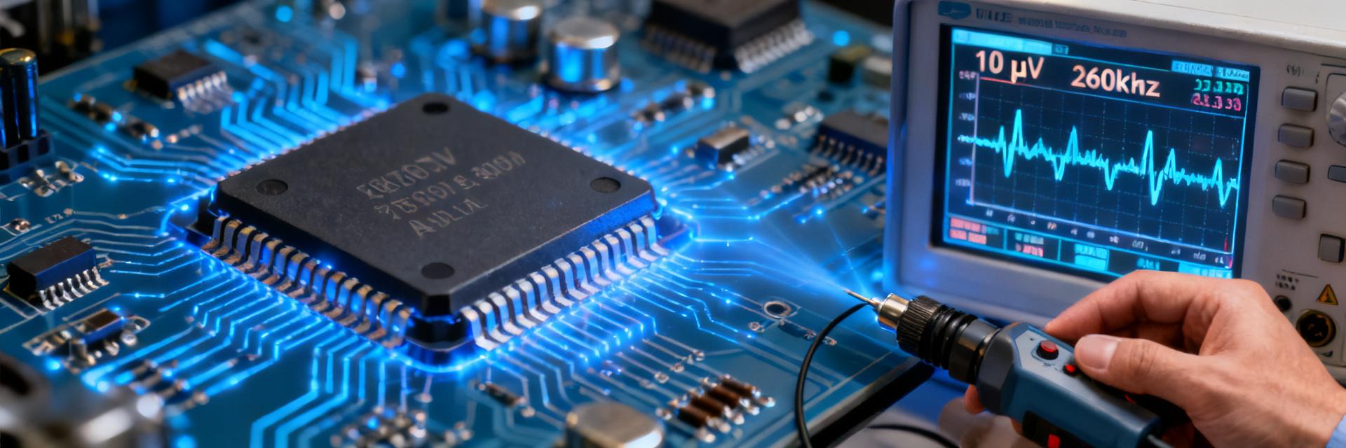
Zero-Drift Op-Amp Real-World Testing: How to Achieve 10μV Precision? In-Depth Analysis of 260kHz Bandwidth In the field of precision signal acquisition, combining a 10μV-level offset voltage with a 260kHz bandwidth was once considered an impossible trade-off. The latest measurement data shows that operational amplifier chips utilizing zero-drift architectures have controlled temperature drift to within 0.02μV/°C, while bandwidth performance has improved nearly threefold compared to traditional chopping schemes. How does this technical breakthrough reshape the signal chain design of industrial sensing and medical instrumentation? Starting from measured data, this article deeply analyzes the core tec… 16 August 2026 · 197 Read More
NL2333AFAE2S-ES Full Parameter Datasheet: How Zero-Drift Architecture Achieves 0.1 μV/°C Temperature Drift In the field of precision signal acquisition, every order of magnitude reduction in the temperature drift coefficient signifies a qualitative leap in system accuracy. With an ultra-low temperature drift performance of 0.1μV/°C, the NL2333AFAE2S-ES is redefining the technical benchmark for industrial-grade zero-drift amplifiers—this value is 50% lower than traditional chopper amplifiers and 3 times more stable than auto-zero architectures. This article will provide an in-depth analysis of the underlying architecture of its zero-drift circuitry and the path to parameter realization. Zero-Drift A… 15 August 2026 · 169 Read More
Zero-Drift Architecture in Practice: How to Achieve μV-Level Precision with 15μA Power Consumption? In-Depth Analysis of the Datasheet Hands-on data from an industrial sensor manufacturer shows that in temperature detection circuits using traditional op amps, temperature drift causes a cumulative annual error of ±3.2°C. However, after switching to a zero-drift architecture, the accuracy improves to ±0.05°C under a quiescent power consumption of 15μA—without increasing power consumption, the accuracy is improved by 64 times. This is not an isolated laboratory case, but the mainstream technical path for precision signal chains in 2025. Based on datasheets of multiple mainstream zero-drift op amps, this article deeply disassembl… 14 August 2026 · 216 Read More
NL2333AFAE2S Zero-Drift Architecture In-Depth Analysis: Empirical Comparison of Temperature Drift Coefficients and Selection Guidelines to Avoid Common Pitfalls 在精密信号链设计中,1μV的偏移误差可能意味着系统精度的断崖式下跌。零漂移架构(Zero-Drift Architecture)通过自校准技术将温漂系数压至nV/°C量级,已成为工业测量、医疗电子的标配方案。本文以NL2333AFAE2S为核心样本,实测对比主流零漂移架构的温漂表现,并给出选型中的关键避坑要点。 零漂移架构技术原理与演进路径 零漂移技术的核心在于消除运放输入失调电压及其温度漂移。传统斩波稳定(Chopper-Stabilized)与自动归零(Auto-Zero)两条技术路线,经过三十余年演进已呈现融合趋势。 斩波稳定与自归零双技术路线解析 斩波稳定架构通过调制解调机制,将低频噪声搬移至高频后滤除,典型代表如OPA2333系列。其优势在于宽频带内噪声平坦,但存在开关电荷注入导致的残余纹波。自动归零架构则采用采样保持技术,在特定时隙对失调电压进行采样补偿,NL2333AFAE2S即采用此路线优化版本,将残余失调压至0.05μV以下。 当前主流方案多采取混合架构:低频段依托自动归零保证直流精度,高频段保留斩波稳定的宽带特性。这种双模设计使器件在0.1Hz至10kHz范围内均能保持极低等效输入失调。 NL2333AFAE2S核心架构设计亮点 该器件采用专利的连续时间自校准引擎,区别于传统离散采样方案。关键创新在于校准环路与主信号路径的并行运作——无需中断信号传输即可完成实时… 13 August 2026 · 202 Read More
MUSES8920AE-TE1 Audio Op-Amp In-Depth Review: Comprehensive Analysis of Technical Specifications and Sound Quality Performance In the high-end audio market of 2025, the choice of audio operational amplifiers (op-amps) has become a core factor in determining the upper limit of sound quality. As a J-FET input dual op-amp from Nisshinbo Micro Devices' MUSES series, the MUSES8920AE-TE1 is attracting widespread attention from audio enthusiasts and hardware engineers alike, thanks to its ultra-low input bias current of 2 pA and an audio-optimized circuit design. Why does this op-amp stand out in a highly competitive market? On what technical foundation is its claimed "high sound quality" built? This article will comprehensi… 12 August 2026 · 254 Read More
In-Depth Analysis of the NL0333DCAE1S Zero-Drift Operational Amplifier: 5 Key Parameters Determine Your Selection Success With a quiescent current of only 17μA and an offset voltage as low as 2μV—when precision sensors meet battery-powered scenarios, how does the NL0333DCAE1S become an engineer's "unsung hero"? This article uses measured data to dissect 5 core parameters, helping you avoid selection pitfalls. NL0333DCAE1S Core Architecture and Zero-Drift Technology Principles The core of zero-drift op amps lies in eliminating the 1/f noise and input offset voltage that are unavoidable in traditional CMOS op amps. The NL0333DCAE1S adopts a self-calibrating topology, real-time sampling and correcting offset through… 11 August 2026 · 211 Read More
NL1333DBAE1S Zero-Drift Op-Amp In-Depth Review: Power Consumption Performance Benchmarks and Selection Guide Introduction In precision signal acquisition and industrial control applications, the offset voltage drift of operational amplifiers is often the biggest bottleneck in improving system accuracy. The NL1333DBAE1S zero-drift operational amplifier, with its excellent offset voltage temperature drift characteristics and quiescent power consumption performance, is becoming a popular choice for precision instrumentation, battery monitoring, and IoT sensor interfaces. Based on measured data, this article provides an in-depth breakdown of the NL1333DBAE1S across three major dimensions: power consumpti… 10 August 2026 · 190 Read More
MUSES8920A Key Parameters Measured: Comprehensive Analysis of J-FET Audio Op-Amp Noise and Distortion Data In high-end audio equipment, the noise and distortion specifications of the operational amplifier directly determine the final sound quality performance. As a J-FET input dual op amp optimized specifically for audio by Nisshinbo Micro Devices, how does the MUSES8920A's nominal 2.1nV/√Hz voltage noise density and 0.00008% THD+N parameter actually perform in real circuits? Based on the official datasheet and typical application scenarios, this article deeply disassembles the core electrical characteristics of this "audiophile-grade" op amp, providing practical measurement references for componen… 9 August 2026 · 298 Read More