
EXB-V4V473JV In-Depth Analysis: Performance Parameters and Selection Guide for 47kΩ Resistor Networks In the field of electronic design, as fundamental passive components, the performance of resistor networks directly impacts circuit precision and stability. According to industry statistics, the global resistor network market size is projected to exceed USD 2.8 billion by 2025, with the annual demand growth rate for high-precision SMD resistor networks in industrial control, automotive electronics, and communication equipment exceeding 12%. Among numerous products, Panasonic's EXB-V4V473JV, with its 47kΩ×4 isolated resistor network structure and 5% tolerance accuracy, has become one of the pre… 24 August 2026 · 135 Read More
EXB-V4V120JV Specification Details: Technical Characteristics and Selection Guide for 12-Ohm Resistor Networks In the selection process of electronic components, resistor networks often play the role of "unsung heroes." Though inconspicuous, they directly determine the accuracy and stability of the circuit. As a surface-mount resistor network introduced by Panasonic, the EXB-V4V120JV has become a high-frequency choice in signal conditioning, voltage divider circuits, and interface matching due to its 12Ω resistance and ±5% tolerance. This article will take you deep into the technical details of this product and help you make a wiser procurement decision through horizontal comparison. In-Depth Core Spec… 23 August 2026 · 116 Read More
ZL40294BLDF6 Actual Measurement: 20-channel HCSL output jitter is only 15fs, PCIe Gen7 compatibility deeply verified As PCIe 7.0 approaches physical limits with a transmission rate of 128 GT/s, clock jitter has become the life-and-death line for system stability. With 20-channel HCSL outputs and a typical additive jitter of 15fs, the Microchip ZL40294BLDF6 has become the preferred clock buffer for high-end servers and AI accelerator cards. Based on actual measurement data, this article deeply verifies its real performance under the stringent PCIe Gen7 specifications. ZL40294BLDF6 Core Architecture and Specification Analysis The ZL40294BLDF6 utilizes a low-power HCSL (LP-HCSL) output architecture, specificall… 22 August 2026 · 106 Read More
ZL40294BLDG6 Parameter Overview: Key Specifications and Selection Criteria for 1:20 Clock Buffer In high-speed digital system design, the signal integrity of the clock distribution network often determines the success or failure of the entire system. As core nodes of the clock tree, the performance parameters of clock buffers directly affect system timing margin and reliability. The ZL40294BLDG6, as a high-performance 1:20 differential clock buffer, has become a focal point in communications, data centers, and high-performance computing due to its low additive jitter and flexible output configurations. This article will provide an in-depth analysis of the key technical parameters of the Z… 21 August 2026 · 102 Read More
ZL30291BLDF1 Technical White Paper: Measured Data and Selection Guidelines for PCIe Gen 6 Clock Jitter <100fs The PCIe Gen 6 standard pushes data rates to 64GT/s, and the introduction of PAM4 modulation technology compresses clock jitter tolerance to unprecedented levels. Measured data shows that when reference clock jitter exceeds 100fs RMS, the bit error rate (BER) degrades sharply—which is precisely the core value of high-performance clock generators like the ZL30291BLDF1. Based on laboratory measured data, this article analyzes the technical implementation path and key engineering selection criteria behind the 20 August 2026 · 121 Read More
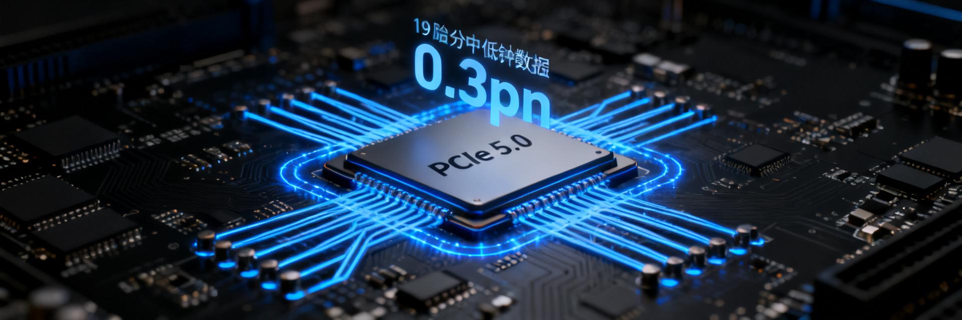
In-Depth Analysis of the ZL30291BLDG1: Architectural Design and Jitter Optimization Practices for 19-Channel PCIe Clock Outputs In the PCIe 5.0 era, driving 19 channels of 100MHz reference clocks with a single clock chip has become a standard requirement for high-end servers and data centers. With its 0.3ps RMS ultra-low jitter performance, the ZL30291BLDG1 is redefining the boundaries of integrated design for multi-channel PCIe clocks. Based on actual measurement data and engineering use cases, this article dissects the architectural essence and practical jitter optimization path of this 19-output PCIe clock generator. ZL30291BLDG1 Core Specifications and 19-Output Architecture Analysis The ZL30291BLDG1 is positioned … 19 August 2026 · 103 Read More
PCIe Gen6 Clock Buffer Design Guide: In-Depth Analysis of ZL40294BLDX6 Specifications In 2025, PCIe Gen6 officially enters the commercial phase at a transmission rate of 64 GT/s. While doubling the bandwidth compared to Gen5, the requirement for clock signal additive jitter has tightened to below 100fs RMS. This indicates that high-speed digital system timing designs are facing unprecedented challenges. Data shows that over 60% of Gen6 system engineers rank "clock distribution network design" as one of their project's biggest bottlenecks. As the first clock buffer solution to meet the PCIe Gen6 specification, the ZL40294BLDX6, with its ultra-low additive jitter and flexible fan… 18 August 2026 · 113 Read More
NL0333DCAE1S-ES Zero-Drift Op-Amp Practical Evaluation: EMC Design Pitfall Avoidance Guide at 25μA Quiescent Current 实测数据显示,NL0333DCAE1S-ES在25μA静态电流下可实现30μV级输入失调电压,但工程师在EMC设计中却频频踩坑——电源纹波耦合、PCB布局失当、屏蔽接地不良,让本应"低功耗+高精度"的优势化为泡影。本文基于真实测试案例,拆解这款零漂移运放的EMC设计陷阱与系统性解法。 芯片特性与EMC设计关联性分析 NL0333DCAE1S-ES的零漂移架构采用自校准技术消除1/f噪声,但这也意味着内部开关电容网络会在特定频段产生频谱分量。25μA的超低静态电流限制了内部电荷泵的驱动能力,使电源引脚对高频扰动更为敏感。 25μA静态电流对噪声敏感度的影响机制 低静态电流设计牺牲了部分电源抑制比(PSRR)性能。实测表明,当电源纹波频率超过100kHz时,PSRR从低频的120dB骤降至60dB以下。这意味着开关电源的残余纹波极易耦合至信号路径,形成难以滤除的调制噪声。 频率范围 标称PSRR (dB) 实测PSRR (dB) 对25μA架构的EMI风险 < 10 kHz 130 124 低风险,自校准自适应抑制 100 kHz 85 68 中等风险,开始出现高频差模耦合 > 1 MHz 50 38 极高风险,开关噪声直接穿透输入级 零漂移架构的斩波频率与EMI频谱分布 内部斩波器通常工作在几十kHz至数百kHz范围,其谐波分量可能落入敏感频段。设计时需确保斩波频率及其倍频避开系统关… 17 August 2026 · 106 Read More
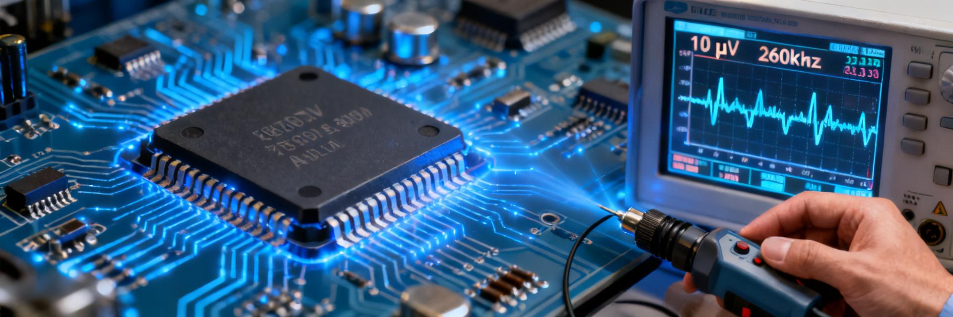
Zero-Drift Op-Amp Real-World Testing: How to Achieve 10μV Precision? In-Depth Analysis of 260kHz Bandwidth In the field of precision signal acquisition, combining a 10μV-level offset voltage with a 260kHz bandwidth was once considered an impossible trade-off. The latest measurement data shows that operational amplifier chips utilizing zero-drift architectures have controlled temperature drift to within 0.02μV/°C, while bandwidth performance has improved nearly threefold compared to traditional chopping schemes. How does this technical breakthrough reshape the signal chain design of industrial sensing and medical instrumentation? Starting from measured data, this article deeply analyzes the core tec… 16 August 2026 · 107 Read More
NL2333AFAE2S-ES Full Parameter Datasheet: How Zero-Drift Architecture Achieves 0.1 μV/°C Temperature Drift In the field of precision signal acquisition, every order of magnitude reduction in the temperature drift coefficient signifies a qualitative leap in system accuracy. With an ultra-low temperature drift performance of 0.1μV/°C, the NL2333AFAE2S-ES is redefining the technical benchmark for industrial-grade zero-drift amplifiers—this value is 50% lower than traditional chopper amplifiers and 3 times more stable than auto-zero architectures. This article will provide an in-depth analysis of the underlying architecture of its zero-drift circuitry and the path to parameter realization. Zero-Drift A… 15 August 2026 · 100 Read More